Dispersion in infinite superlattices: Minibands (Kronig-Penney model)
- Input files:
1Dsuperlattice_dispersion_4nm_nnpp.in
1Dsuperlattice_dispersion_6nm_nnpp.in
1Dsuperlattice_dispersion_bulk_GaAs_nnpp.in
Superlattice_1D_nnpp.in
- Scope:
This tutorial aims to reproduce two figures (Figs. 2.27, 2.28, p. 56f) of [HarrisonQWWD2005], thus the following description is based on the explanations made therein.
Superlattice 1: 4 nm
Input file: 1Dsuperlattice_dispersion_4nm_nnpp.in
Our infinite superlattice consists of a 4 nm
Figure 2.4.279 shows the conduction band edge and the first eigenstate that is confined inside the well and its corresponding charge density (
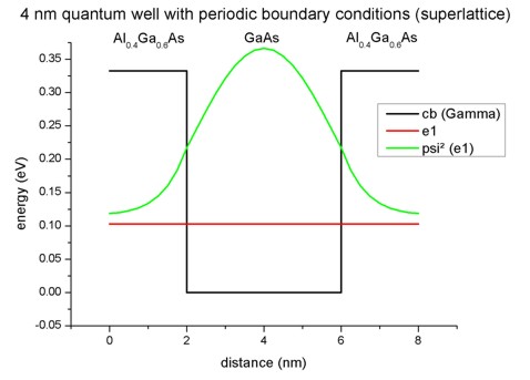
Figure 2.4.279 Calculated conduction band edge profile of single 4 nm GaAs QW with periodic boundary conditions.
In a superlattice the electrons (and holes) see a periodic potential which is similar to the periodic potential in bulk crystals. This means that the particle wave functions are no longer localized in one quantum well. They extend to infinity, and they are equally likely to be found in any of the quantum wells. The eigenstates are called Bloch states (as in bulk) and the wave functions are periodic:
For a travelling wave of the form
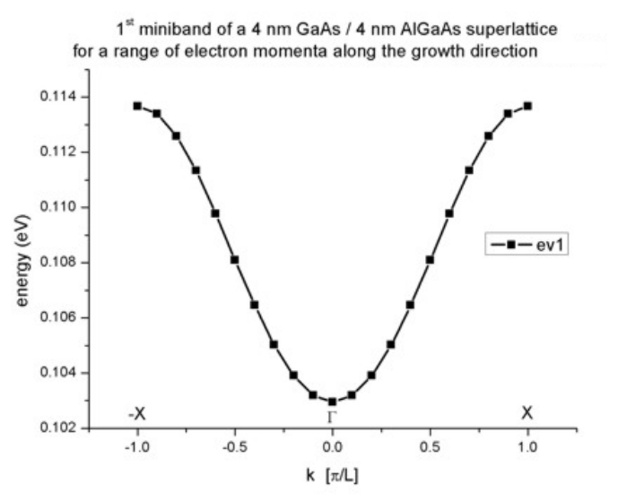
Figure 2.4.280 Calculated subband dispersion (= miniband)
The plot is in excellent agreement with Fig. 2.27 (page 56) of [HarrisonQWWD2005].
When the electron is at rest (
Superlattice 2: 6 nm
Input file: 1Dsuperlattice_dispersion_6nm_nnpp.in
Our second infinite superlattice consists of a 6 nm
Figure 2.4.281 shows the conduction band edge and the two lowest eigenstates that are confined inside the well and their corresponding probailiy density (
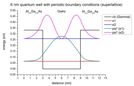
Figure 2.4.281 Calculated conduction band edge profile of single 6 nm
The following figure (Figure 2.4.282) shows the first two minibands for this superlattice. They arise from the first and the second eigenstate. Note that due to the scale of this figure the first miniband looks almost flat. It is also interesting that for the second miniband the minimum is not at the center (i.e. at Gamma) but at the edges of the superlattice Brillouin zone at X (and -X).
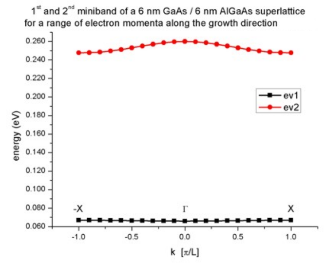
Figure 2.4.282 Calculated subband dispersion (= miniband)
Again, the plot is in excellent agreement with Fig. 2.28 (page 57) of [HarrisonQWWD2005].
Technical details
The resolution of the miniband plot has to be specified within the group quantum{ region{ dispersion{} } }:
quantum{
    region{
        ...
        dispersion{
            output_dispersions{}
            path{
                name = "superlattice_dispersion"
                point{ k = [$left_dispersion,  0.0, 0.0] }
                point{ k = [$right_dispersion, 0.0, 0.0] }
                num_points = $num_points_dispersion         # number of superlattice vectors along x direction
            }
        }
    }
}
For each superlattice vector
Dispersion in bulk
Input file: 1Dsuperlattice_dispersion_bulk_GaAs_nnpp.in
The input file is basically equivalent to 1Dsuperlattice_dispersion_6nm_nnpp.in, except that we replace the
Figure 2.4.283 shows the conduction band edge and the three lowest eigenstates and their corresponding probability density (
The ground state wave function is constant with its energy equal to the conduction band edge energy.
The energies of the second and third eigenstate are degenerate.
(Note that the energies were shifted so that the conduction band edge of
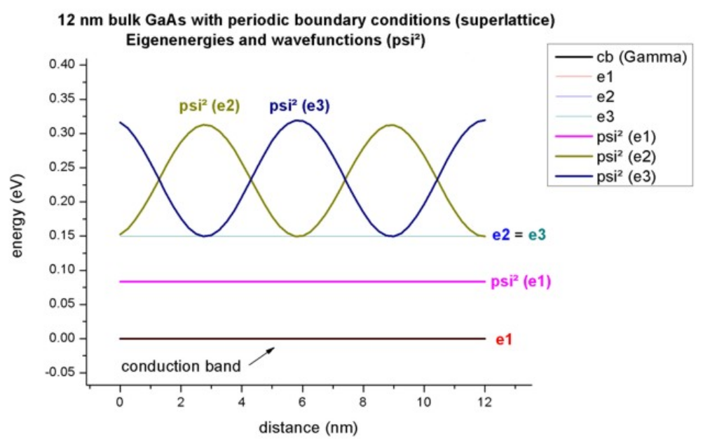
Figure 2.4.283 Calculated conduction band edge profile of bulk
The following figure (Figure 2.4.284) shows the first three minibands for this superlattice. They arise from the first, second and third eigenstate.
The second and third eigenstate are degenerate at
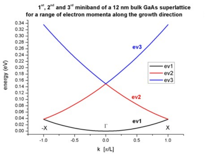
Figure 2.4.284 Calculated subband dispersion (= miniband)
Template
Input file: Superlattice_1D_nnpp.in
We want to study the energy levels of a superlattice in order to understand how they form bands in a periodic structure. One can easily see this by calculating the energy levels for various barrier heights, i.e. we automatically generate input files for the variable “Barrier_Height”. Once done, we visualize the subband dispersions contained in the file dispersion_quantum_region_Gamma_superlattice_dispersion.dat.
Figure 2.4.285 compares the dispersion of a superlattice for two different QW barrier heights.
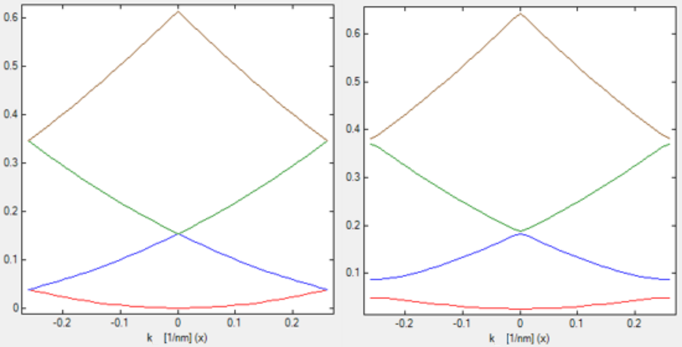
Figure 2.4.285 The left figure contains a quantum well superlattice with a barrier height of 0 eV, i.e. a bulk semiconductor, while the figure on the right shows the dispersion for a barrier height of 0.06 eV.
Last update: nn/nn/nnnn