— DEV — I–V characteristics of n-doped Si structure
- Input files:
I-V_n-doped-Si_1D_nnp.in
I-V_n-doped-Si_2D_nnp.in
I-V_n-doped-Si_3D_nnp.in
I-V_nin-doped-Si_1D_nnp.in
I-V_nin-doped-Si_2D_nnp.in
I-V_nin-doped-Si_3D_nnp.in
- Scope:
This tutorial aims to simulate the I-V characteristics of n-doped and n-i-n doped Si structures.
- Output files:
IV_characteristics.dat
bias_xxxxx/bandedges.dat
I-V characteristics of an n-doped Si structure
Structure
The structure we are dealing with consists of bulk Si that is sandwiched between two contacts. The whole structure has the following dimensions (see also):
along
-axis: ( contact, Si, contact) along
-axis:
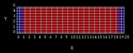
Figure 2.4.50 Simulated structure consisting of a left and right contact (blue) and n-doped Si layer (red).
The Si is n-type doped with a donor concentration of
For the effective electron mass at the
where
The effective density of states reads:
where the factor of 12 arises due to the six-fold degeneracy of Si at
Note that heavy and light holes are degenerate for
The Semiconductor equation is given by
with
The occupation of the different energy states can either be described by Maxwell-Boltzmann statistics:
or Fermi-Dirac statistics:
where
When using the Maxwell-Boltzmann statistics as an approximation, we obtain:
Note that nextnano++ uses the Fermi-Dirac integrals (Fermi-Dirac statistics), where the following results are obtained:
Results
We sweep the voltage at the right contact from
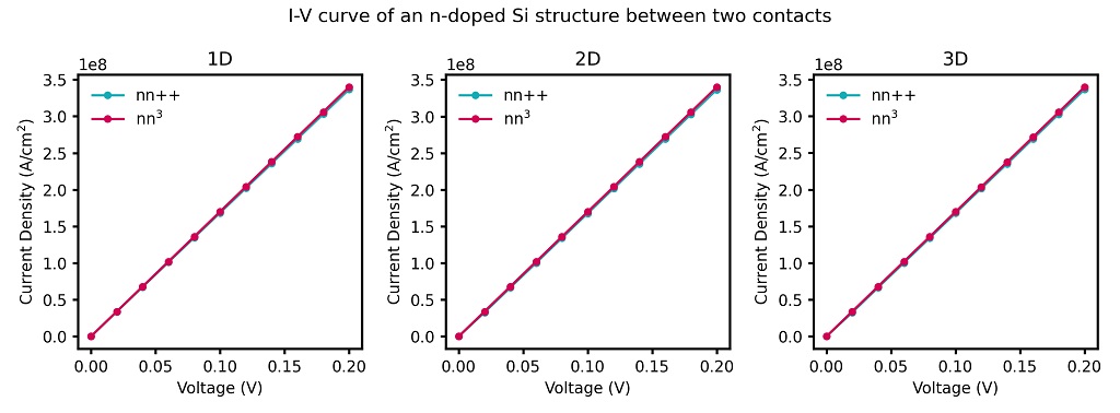
Figure 2.4.51 Simulated I-V characteristics of an n-doped Si structure using constant mobility model.
The nextnano++ results are in agreement with the I-V characteristics obtained with nextnano³. The units for the current in a 2D simulation are [
I-V characteristics of an n-i-n-doped Si structure
Structure
The second example is an n-i-n (n-doped, intrinsic, n-doped) Si structure, which is shown in Figure 2.4.52. The width of the intrinsic region is 14 nm, and the n-doped regions are both 2 nm wide.
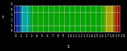
Figure 2.4.52 Simulated n-i-n structure consisting of a left contact (dark blue), n-doped Si (light blue), intrinsic Si (green), n-doped Si (yellow) and right contact (red).
Results
In Figure 2.4.53 the current-voltage (I-V) characteristic is shown. The input files used for the simulations are I-V_nin-doped-Si_1D_nnp.in, I-V_nin-doped-Si_2D_nnp.in I-V_nin-doped-Si_3D_nnp.in. The data of the I-V curve can be found in the corresponding file IV_characteristics.dat.
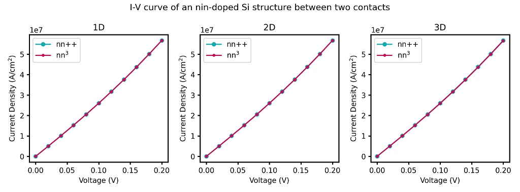
Figure 2.4.53 Simulated I-V characteristics of the n-i-n doped Si structure using constant mobility model.
In order to compare the results from 1D, 2D and 3D simulations, we have divided the 2D current by the width of the device (in our case 5 nm) and the 3D current by the cross-section area of the device of (in our case
Figure 2.4.54 shows the conduction band profile (bias_xxxxx/bandedges.dat) for different voltages.
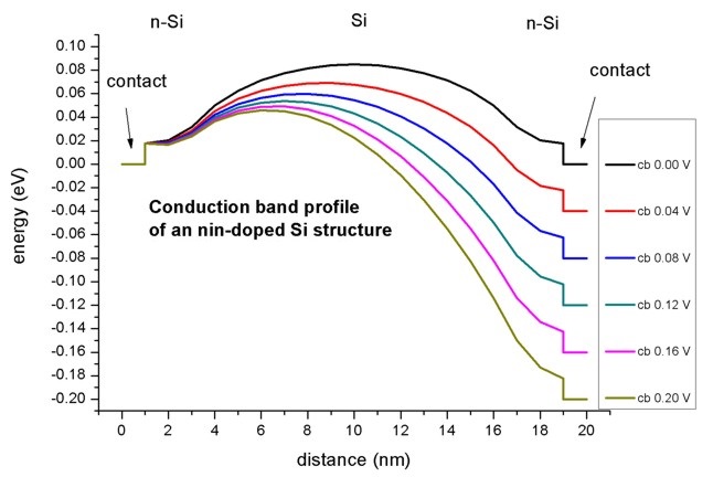
Figure 2.4.54 Simulated conduction band profile of the n-i-n Si structure for different voltages.
Last update: 17/07/2024