Si/SiGe MODQW (Modulation Doped Quantum Well)
- Input files:
1DSiGe_Si_Schaeffler_SemicondSciTechnol1997_nnpp.in
- Scope:
This tutorial aims to reproduce Fig. 11 of [Schäffler1997].
Introduction
Layer sequence
width [nm] |
material |
strain |
doping [cm-3] |
|
1 |
Schottky barrier 0.8 eV |
|||
2 |
15.0 |
Si cap |
strained w.r.t Si0.75 Ge0.25 |
|
3 |
22.5 |
Si0.75 Ge0.25 layer |
||
4 |
15.0 |
Si0.75 Ge0.25 doping layer |
2 |
|
5 |
10.0 |
Si0.75 Ge0.25 barrier |
||
6 |
18.0 |
Si channel |
strained w.r.t Si0.75 Ge0.25 |
|
7 |
69.5 |
Si0.75 Ge0.25 buffer |
Material parameters
The material parameters were taken from [Schäffler1997]. The temperature was set to 0.1 K. The Si layers are strained pseudomorphically with respect to a Si0.75 Ge0.25 substrate (buffer layer).
Method
Self-consistent solution of the Schrödinger-Poisson equation within single-band effective-mass approximation (using ellipsoidal effective mass tensors) for both Delta conduction band edges.
Results
Figure 2.4.130 shows the self-consistently calculated conduction band profile and the lowest wave functions of an n-type Si/Si0.75 Ge0.25 modulation doped quantum well (MODQW) grown on a relaxed Si0.75 Ge0.25 buffer layer. The strain lifts the sixfold degeneracy of the lowest conduction band (Delta6) and leads to a splitting into a twofold (Delta2) and a fourfold (Delta4) degenerate conduction band edge.
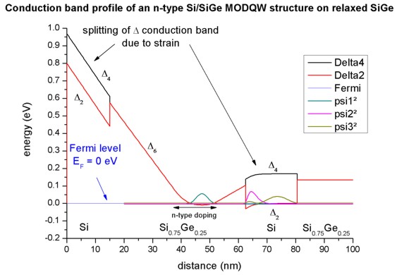
Figure 2.4.130 Calculated conduction band edge profile.
Figure 2.4.131 shows the lowest three wave functions (
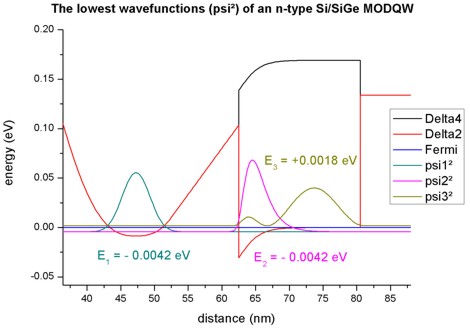
Figure 2.4.131 Calculated probability densities of the lowest electron states.
The electron density (in units of 1
in the parasitic Si0.75 Ge0.25 channel: 0.75
1012 cm-2. in the strained Si channel: 0.66
1012 cm-2.
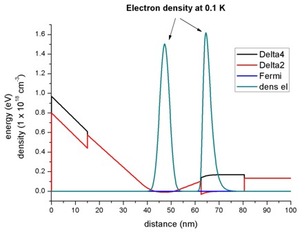
Figure 2.4.132 Calculated electron density profile.
Last update: nn/nn/nnnn