Single-electron transistor - laterally defined quantum dot
- Input files:
SET_Scholze_IEEE2000_1D_nnpp.in
SET_Scholze_IEEE2000_3D_cl_nnpp.in
SET_Scholze_IEEE2000_3D_top_gates_cl_nnpp.in
Note
If you want to obtain the input files that are used within this tutorial, please check if you can find them in the installation directory. If you cannot find them, please submit a Support Ticket.
- Scope:
In this tutorial, we simulate an
/ heterostructure grown along the z direction. The tutorial is based on [Scholze2000].
Introduction
The
Figure 2.4.523 shows the conduction band edge
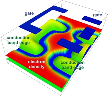
Figure 2.4.523 Conduction band edges (green), electron density (red) and geometry of the top gates (blue).
We divide the tutorial into two parts:
In part 1, we simulate the heterostructure along the
In part 2, we solve the 3D Poisson equation to study the effect of the gates. (3D simulation: only Poisson equation using a classical density), SET_Scholze_IEEE2000_3D_top_gates_cl_nnpp.in
Part 1: 1D simulation (self-consistent Schrödinger-Poisson)
Figure 2.4.524 shows the calculated conduction band edge and the electron density of the heterostructure. The results are similar to Fig. 4 in [Scholze2000].
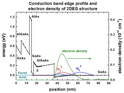
Figure 2.4.524 Conduction band edge profile (black), electron density (green) and Fermi levels (cyan) of 1D simulation.
At the left boundary, a Schottky barrier of 0.6 V has been assumed.
At
Part 2: 3D simulation with top gates (Poisson equation only)
Figure 2.4.525 shows the 3D structure that we are going to simulate.
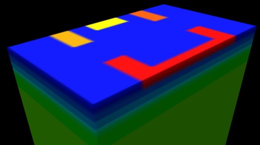
Figure 2.4.525 Device structure (3D)
Figure 2.4.526 shows two 2D slices through the lateral
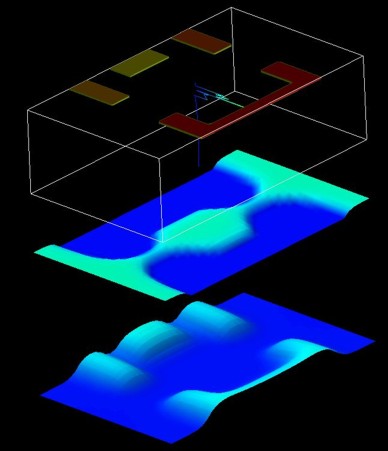
Figure 2.4.526 In the middle, the electron density is shown. The electron density has been calculated classically. At the bottom, the conduction band edge is shown.
Last update: nnnn/nn/nn