Energy dispersion of holes in a quantum well
- Input files:
1Dwell_GaAs_AlAs_nnp.in
1Dwell_GaSb_AlSb_nnp.in
1Dwell_InGaAs_InP_nnp.in
- Scope:
In this tutorial we aim to reproduce results of [FranceschiJancuBeltram1999] and [Holleitner2007].
a) Unstrained
Input file: 1Dwell_GaAs_AlAs_nnp.in
This input file simulates a
Figure 2.4.255 shows the valence band edges of the quantum well structure together with three quantized states. The heavy and light hole band edges are degenerate. The red band is the split-off hole band edge. Note that these artificial band edges correspond to the bulk band edges.
Also shown are the probability densities of the three uppermost subbands (
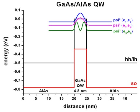
Figure 2.4.255 Calculated valence band edges with
We use a 6-band k.p model for the holes.
quantum {
    region{
        name = "quantum_region"
        x = [10, 34.8]
        no_density = yes
        boundary{ x = dirichlet }
        kp_6band{ # 6-band k.p model
            num_ev = 10 # number of hole states
            dispersion{
                ...
            }
            k_integration{
                ...
            }
        }
        output_wavefunctions{ # k.p output
            max_num = 9999
            all_k_points = yes
            amplitudes = no
            probabilities = yes
        }
    }
}
Database: We used the Luttinger parameters (
database{
    binary_zb{
        name    = AlAs
        valence = III_V

        valence_bands{
            bandoffset = 0.86633 # Ev,av [eV]
        }

        kp_6_bands{     # Dresselhaus parameters
            L = -7.64   # [hbar^2/2m]
            M = -3.50   # [hbar^2/2m]
            N = -8.76   # [hbar^2/2m]
        }
    }

    binary_zb{
        name    = GaAs
        valence = III_V

        valence_bands{
            bandoffset = 1.346 # Ev,av [eV]
        }

        kp_6_bands{     # Dresselhaus parameters
            L = -16.050 # [hbar^2/2m]
            M = -4.050  # [hbar^2/2m]
            N = -18.000 # [hbar^2/2m]
        }
    }
}
The valence band offset between
The eigenvalues are twofold degenerate due to spin (and because the quantum well is symmetric). Thus, eigenvalue 1 and 2 correspond to Figure 2.4.256, 3 and 4 to Figure 2.4.257 and 5 and 6 to Figure 2.4.258.
For the following three pictures, the energy is referred to the bulk valence band edge of the quantum well material, i.e. hh/lh(
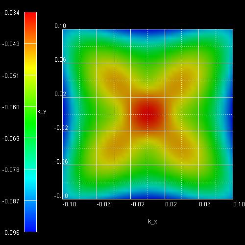
Figure 2.4.256 Subband 1 (eigenvalue 1 and 2)
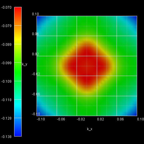
Figure 2.4.257 Subband 2 (eigenvalue 3 and 4)
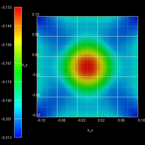
Figure 2.4.258 Subband 3 (eigenvalue 5 and 6)
Now we will plot a cut through the above three pictures from [010] to the zone center and from the zone center to [011], see Figure 2.4.259. This plot was obtained by plotting the following file: dispersion_quantum_region_kp6_kpar_10_00_11.dat.
The value of the abscissa is found as follows:
From [10] to zero we just take
. From zero to [11] we take
.
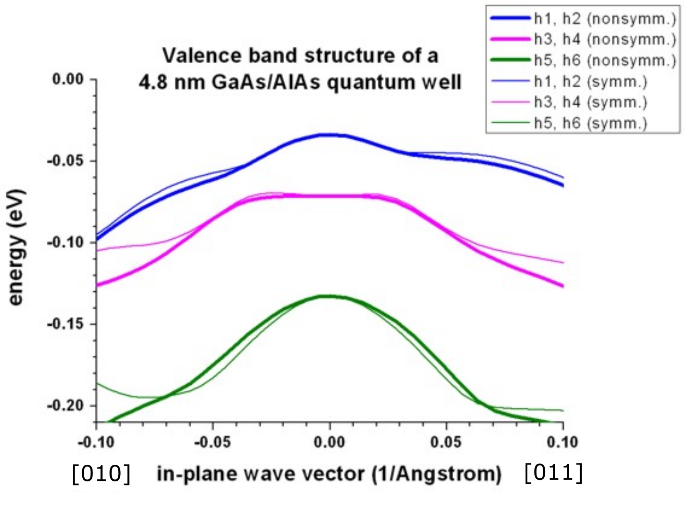
Figure 2.4.259 Calculated valence band structure of a
The above figure shows the eigenvalues as a function of
Symmetrized vs. nonsymmetrized k.p Hamiltonian
Note
In nextnano++ the symmetrized k.p Hamiltonian is not implemented. Only nextnano³ allows switching between the k.p dispersion for the nonsymmetrized and symmetrized k.p Hamiltonian by an explicit keyword.
$numeric-control
 simulation-dimension           = 1
 kp-vv-term-symmetrization      = no   ! nonsymmetrized k.p Hamiltonian
!kp-vv-term-symmetrization      = yes  !     symmetrized k.p Hamiltonian
b) Tensely strained
Input file: 1Dwell_GaSb_AlSb_nnp.in
Figure 2.4.260 reproduces Fig. 2 of [FranceschiJancuBeltram1999] very well.
It is a tensely strained 5.1 nm
The figure shows that the first two subbands are nearly degenerate at the Brillouin zone center and show strong coupling.
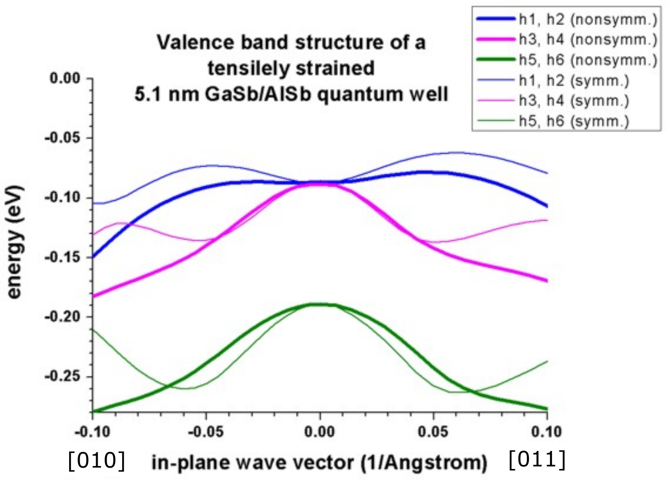
Figure 2.4.260 Calculated valence band structure of a tensely strained
A large discrepancy between the nonsymmetrized and the symmetrized k.p Hamiltonian can be seen. (See also the discussion in [FranceschiJancuBeltram1999] and their tight-binding results.)
c) Tensely strained
Input file: 1Dwell_InGaAs_InP_nnp.in
The following figure reproduces Fig. 3 of [FranceschiJancuBeltram1999] very well.
It is a tensely strained 5.7 nm
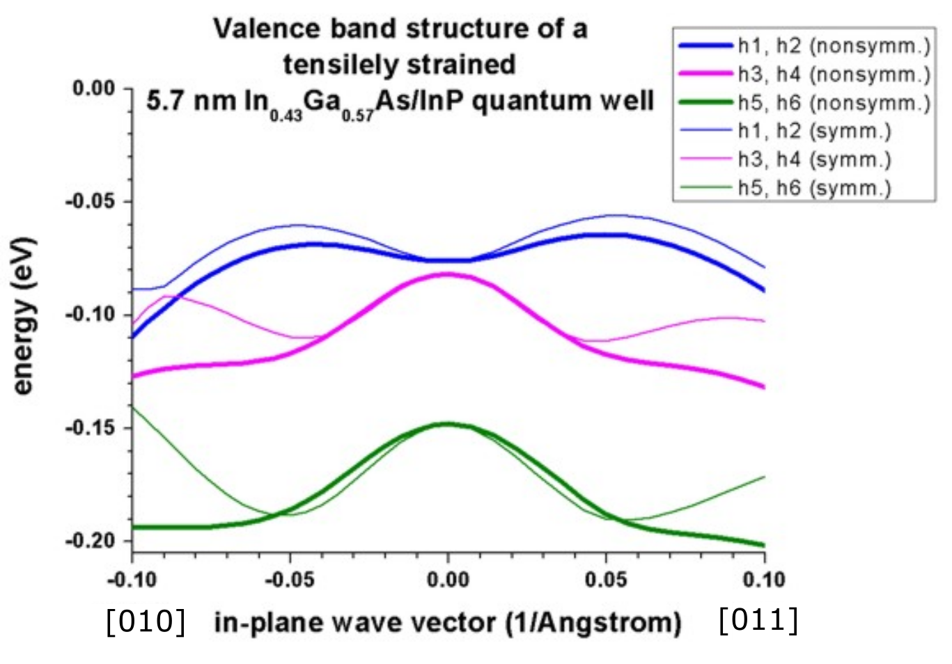
Figure 2.4.261 Calculated valence band structure of a tensely strained
Again, a large discrepancy between the nonsymmetrized and the symmetrized k.p Hamiltonian can be seen. (See also the discussion in [FranceschiJancuBeltram1999] and their tight-binding results.)
d) Strained
Input files:
1DIn20Ga80AsQW_75nm_sg.in
1DIn20Ga80AsQW_75nm_kp.in
1DIn20Ga80AsQW_75nm_kp_dispersion.in
These input files have been used for Fig. 8 in the following paper: [Holleitner2007].
1DIn20Ga80AsQW_75nm_sg.in
A 7.5 nm
The
Consequently, we first have to solve the single-band Schrödinger equation together with the Poisson equation self-consistently, in order to obtain the electrostatic potential. The electron ground state is below the Fermi level.
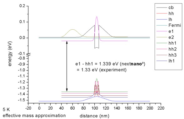
Figure 2.4.262 Calculated band edge profile of a compressively strained
1DIn20Ga80AsQW_75nm_kp.in
The calculated electrostatic potential is read in and then the 8-band k.p equation is solved to get the eigenstates for
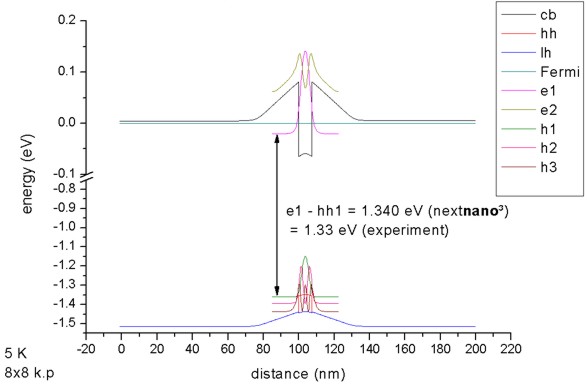
Figure 2.4.263 Calculated band edge profile of a compressively strained
For
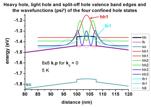
Figure 2.4.264 Calculated valence band structure and lowest hole states of a compressively strained
1DIn20Ga80AsQW_75nm_kp_dispersion.in
We read in the electrostatic potential again and calculate the 8-band k.p dispersion for
For
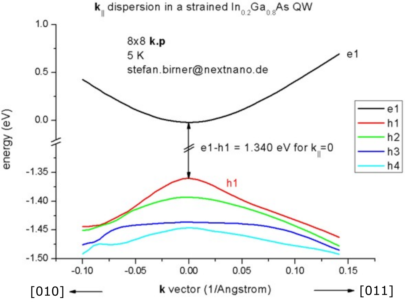
Figure 2.4.265 Calculated subband dispersions in
Figure 2.4.266 shows the
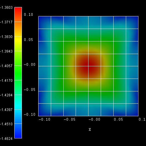
Figure 2.4.266 Calculated dispersion of h1 state in a
Last update: nnnn/nn/nn