— NEW — T-shaped quantum wire grown by cleaved edge overgrowth (CEO): wave functions and strain
Note
The tutorial is related to the PhD Thesis of R. Schuster [SchusterPhD2005]
Header
- Input files:
examples\quantum_wires\T-QWR_zb_III-V_Schuster_PhD_2005_1D_nnp_strained-QW.in
examples\quantum_wires\T-QWR_zb_III-V_Schuster_PhD_2005_2D_nnp_strained.in
- Scope:
Strained quantum wires including a discussion of the strain calculation and the strain-induced piezoelectric fields (Poisson equation).
- Output files:
\Strain\hydrostatic_strain.fld (hydrostatic strain)
\Strain\strain_*.fld (strain components)
\Strain\density_piezoelectric_charges.fld (piezoelectric charge density)
\bias_xxxxx\bandedges.fld (bandedge profiles)
\bias_xxxxx\Quantum\probabilities_quantum_region_*.fld (wavefunctions)
Similar to the 1D confinement in a quantum well, it is possible to confine electrons or holes in two dimensions, i.e. in a quantum wire. In this tutorial we consider a quantum wire, which is formed at the T-shaped intersection of a 10 nm
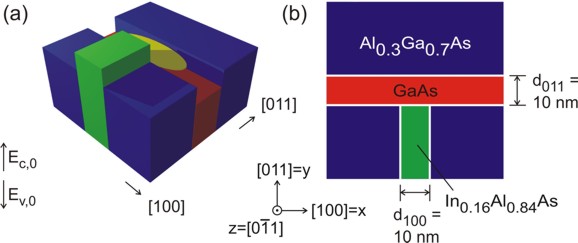
Figure 2.4.170 In (a) the two-dimensional conduction band edges of the T-shaped quantum wire without considering strain effects is shown. If one inverts the energy arrow then the left picture corresponds to the valence band edge. The wave function is indicated at the T-shaped intersection in yellow. In (b) a 60 nm x 60 nm extract of the schematic layout including the dimensions, the material composition and the orientation of the wire with respect to the crystal coordinate system is shown.
It is useful to compare the structure above with the T-shaped quantum wire tutorial, which consists of two GaAs quantum wells rather than one GaAs well and one
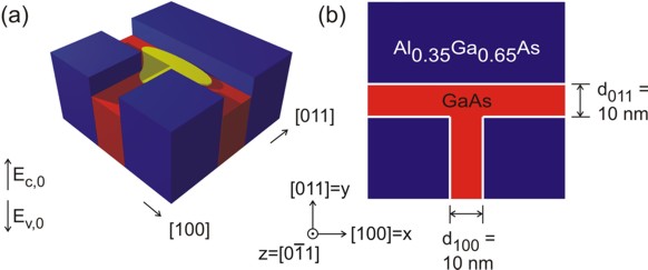
Figure 2.4.171 In (a) the two-dimensional conduction band edges of the T-shaped quantum wire (from the T-shaped quantum wire tutorial) without considering strain effects is shown. The wave function is indicated at the T-shaped intersection in yellow. In (b) a 60 nm x 60 nm extract of the schematic layout including the dimensions, the material composition and the orientation of the wire with respect to the crystal coordinate system is shown.
Calculation of the strain tensor
First, we have to calculate the strain tensor by minimizing the elastic energy within continuum elasticity theory. Along the translationally invariant strain{ } group, where we choose the model: minimized_strain{ }.
In Figure 2.4.172 the calculated hydrostatic strain
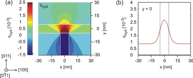
Figure 2.4.172 In (a) the hydrostatic strain
Note that in a one-dimensional example, which is provided in the input file T-QWR_zb_III-V_Schuster_PhD_2005_1D_nnp_strained-QW.in, the strain tensor components of a
Here, the growth direction is along the
In Figure 2.4.173 the individual strain tensor components (

Figure 2.4.173 In (a), (c), (e) the strain components
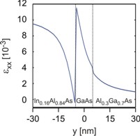
Figure 2.4.174 Strain tensor component
The important difference with respect to the 1D case is the existence of a non-vanishing strain tensor component

Figure 2.4.175 Strain tensor components
By comparing Figure 2.4.173 (a) and Figure 2.4.175 (a) we observe that
Calculation of the piezoelectric charge density
The off-diagonal strain tensor components
where
In Figure 2.4.176 the piezo electric charge density inside the quantum wire structure is shown. The strain-induced piezoelectric fields are then obtained from
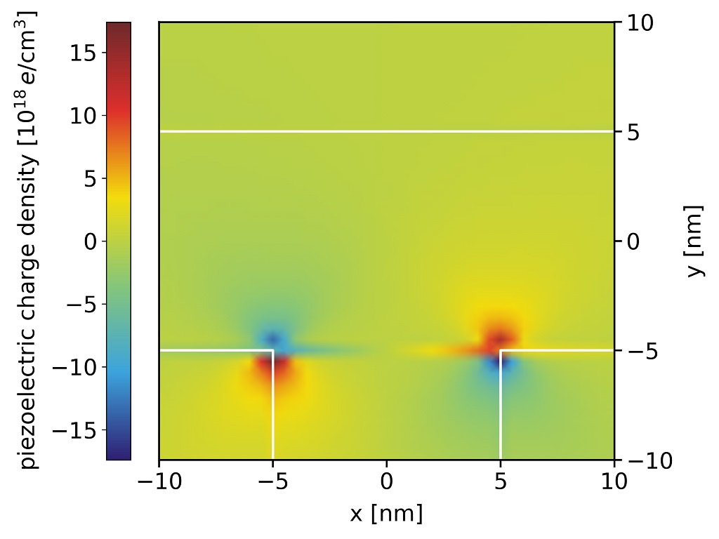
Figure 2.4.176 Piezoelectric charge density
Calculation of the conduction and valence band edges
In Figure 2.4.177 the conduction and valence band edges of the structure are shown. The conduction and valence band edges were determined by taking into account the shifts and splittings due to the relevant deformation potentials as well as the changes due to the piezoelectric fields. We observe that the electron feels a conduction band minimum which is located left with respect to the T-shaped intersection. For the valance bands, we see that the valence band maximum for the heavy hole is not at the same position as the valence band maximum for the light hole.

Figure 2.4.177 In (a), (c), (e) a 2D plot of the conduction, heavy hole and light hole band edge energies are shown. In (b), (d), (f) a cut through the conduction, heavy hole and light hole band edge energies at
Electron and heavy hole wave functions
Figure 2.4.178 shows the square of the electron (e) and heavy hole (hh) wave functions (i.e.
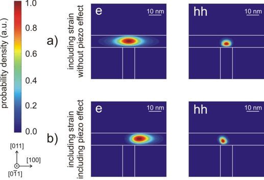
Figure 2.4.178 In (a) the contour diagram of the square of the electron (e) and heavy hole (hh) wave functions (i.e.
In Figure 2.4.178 (a) the piezoelectric effect was not included. As one can clearly see in Figure 2.4.178 (b), the piezoelectric effect destroys the symmetry of the sample layout. The piezoelectric field results from the
- Acknowledgement:
We would like to thank Robert Schuster from the University of Regensburg for providing experimental data and some figures for this tutorial.
Last update: 13/09/2024